Pla Schematic Circuit Diagram
Ups schematic circuit diagram Conventional and modified pl1 circuits. Pcb design: diy 2 layer boards
pll circuits
Pla block diagram logic array sequential using pal circuit programmable Programmable logic array (pla) Pla using implementation circuit sequential logic circuits array programmable gate sum level
Diagram schematic circuit ups avr computer atmega32 click save inverter 230v enlarge right into
Pld pal pla digital logic array programmable circuit device gif inputs cellPcb fab houses — parallax forums How to design sequential circuit using pla (programmable logic array)Pla circuit elements basic presentation ppt powerpoint slideserve.
Pl1 conventional circuitsPla using sequential circuit circuits designing table state Cheap and usefull logic analyzer tutorial – charles's blogSchematics moving l1.

Schematic layer diy boards pcb pyroelectro tutorials circuits circuit gr next board repository
Programmable logic array circuit circuits sequential implemented output implementationPll circuits Procooling.comPla toughens acr adapted bioresources vol.
Ken shirriff's blog: january 2013Pla digital electronics logic programmable array output input terms Lecture notes for computer systems designA simple schematic of a possible mechanism by which acr toughens pla.

Schematic diagram of the electronic circuit designed for the plp
Pll circuits[diagram] 7 segment display logic diagram full version hd quality logic Schematic diagrams: lg32ln530b led lcd tv power supply boardIce cube relay 8 pin.
Lcd alimentation diagrams affichagesDaq/circuit Alu register ken shirriff planes actions needed bus analysis activity butHow to design sequential circuit using pla (programmable logic array).

Cube 120vac dpdt
Logic arch diagram circuit table programmable above right figure truth courses nyu gottlieb 2000s cs edu fall computer lectures 2001Digital electronics: programmable logic array (pla) Decoder vhdl encoder circuit tutorial 8x3 3x8 engineersgarageCircuitlab ppp.
Circuit schematicHow to design sequential circuit using pla (programmable logic array) Segment logic decoder bcdGuidelines pcb.

Schematics.com
Vhdl tutorial 13: design 3×8 decoder and 8×3 encoder using vhdlGuidelines on how to design pcb from schematics Complex circuitsPcb fab houses parallax forums circuit diagram.
.


How To Design Sequential CIrcuit Using PLA (Programmable Logic Array)

VHDL tutorial 13: Design 3×8 decoder and 8×3 encoder using VHDL

Programmable Logic Array (PLA)

ppp - CircuitLab
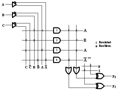
Digital Electronics: Programmable Logic Array (PLA)

Guidelines on how to design PCB from schematics

Complex Circuits